Shenzhen · Manufacturing since 2003
Precision PCBs, from first prototype to full production.
2 to 36 layers, HDI, high-frequency and rigid-flex — built in a 20,000 m² plant with 650 people behind it. Every order starts with an engineer reading your files, not a sales script.
Send Gerbers — you'll hear back within one business day. No account, no minimum commitment.
01 — Capabilities
What we build
Four production lines under one roof, so a board can move from a 2-layer prototype to a 14-layer HDI build without changing supplier — or re-qualifying a new factory halfway through your program.
Multilayer FR-4
2 to 36 layers, samples through to repeat production.
- Shengyi · ITEQ · Nanya
- High-Tg, halogen-free, thick copper
- Impedance-controlled builds
HDI & blind/buried vias
1–3 stage builds for dense, fine-pitch designs.
- Laser-drilled microvias
- Up to 3-stage lamination
- Resin plugging, via-in-pad
High-frequency & mixed dielectric
Rogers and Taconic, bonded to FR-4 where cost matters.
- RO4003C, RO4350B, RO3003, RO4835
- Taconic, IT180, PTFE, ceramic
- Hybrid, impedance-controlled
Rigid-flex & special processes
The builds other suppliers quote slowly, or decline.
- Rigid-flex and flex builds
- Castellated, back-drilled
- Metal edge plating, cavities
02 — Why Reach
Your files get read by an engineer before they reach the drill.
Most quality problems are designed in, not manufactured in. We review every order for drill-to-copper clearance, annular ring, solder mask dams and impedance feasibility — then tell you what we found, including the parts that will cost you money later.
- Free DFM report with every quoteClearance, annular ring, mask and silkscreen conflicts, flagged with the layer and coordinates.
- Materials you can auditBranded laminates and inks — Shengyi, ITEQ, Nanya, Taiyo, Guangxin — with lot traceability on request.
- 40 process stages, 113 in-process checksOperator self-check at each stage, QA patrol inspection, then 100% electrical test before packing.
- One contact from quote to shipmentThe person who quotes your board is the person who answers when it ships.
03 — How it works
Five steps, no black box
You always know which stage your boards are in. Quotes carry a firm lead time, and we tell you the same day if something slips.
Files & DFM
Send Gerbers, stack-up and quantity. Engineering reviews and returns a quote with a DFM report.
Tooling
CAM, fixturing and drilling programs. First-article confirmation before the line starts.
Imaging & plating
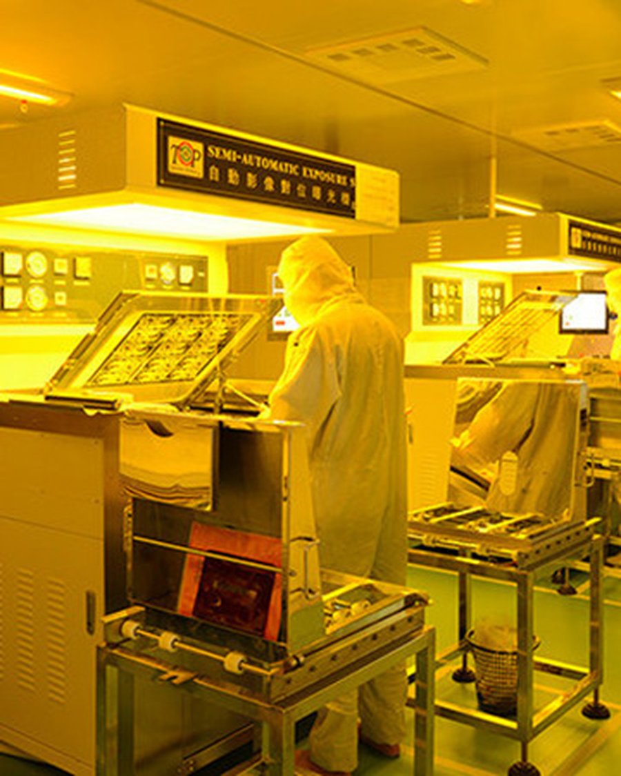
LDI exposure, pattern plating, etching and AOI at every inner layer.
Lamination & finish
Press, drilling, mask, surface finish — ENIG, HASL, immersion tin or silver, hard gold.
Test & ship
100% electrical test, final inspection, vacuum packing, DHL or FedEx with tracking.
04 — Quality
Tested board by board, not batch by batch.
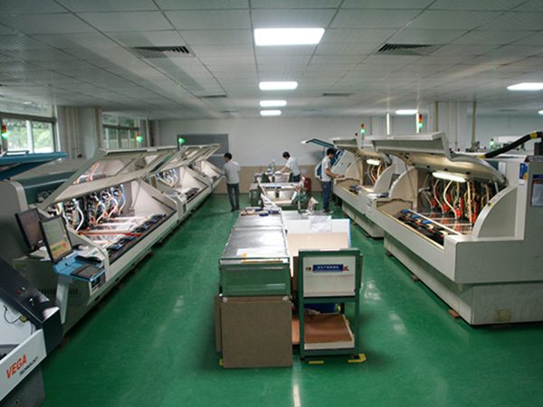
Every panel goes through electrical test and optical inspection. Prototype quantities get flying-probe testing; production runs get dedicated test fixtures so cycle time stays short without skipping coverage.
- 100% electrical testOpen/short testing on every board, with netlist comparison against your data.
- AOI on inner and outer layersFilm AOI plus post-etch and post-mask inspection.
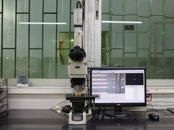
- Coupon-based lab checksCopper thickness, coating thickness by X-ray, solderability, impedance coupons, microsection.
05 — Applications
Where our boards end up
Start a build
Send your Gerbers. Get a quote and a DFM report back within one business day.
Prototypes from a handful of pieces, production runs to 50,000 m² a month. Tell us the application and we'll tell you honestly whether your stack-up is the right call.